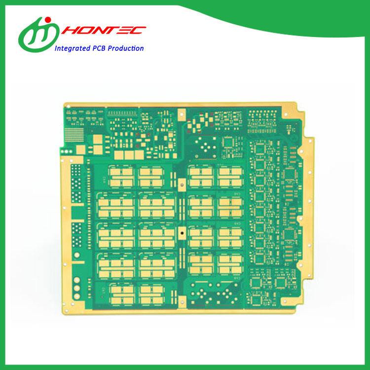
The Manufacturing Process of a Multilayer Board: A Step-by-Step Guide
2024-05-24
Multilayer boards, also known as multilayer printed circuit boards (PCBs), are a crucial component in modern electronics. They enable the integration of complex circuitry in a compact and efficient manner. In this blog, we'll explore the key steps involved in the manufacturing process of a multilayer board.
Step 1: Design and Layout
The manufacturing process begins with the design and layout of the multilayer board. Engineers use CAD (computer-aided design) software to create the schematic diagram and layout of the board, specifying the location of components, traces, vias, and other features. The design takes into account factors like electrical performance, thermal management, and mechanical considerations.
Step 2: Material Selection
Based on the design requirements, the appropriate materials are selected for the various layers of the board. This includes copper foil for the conductive layers, dielectric substrates (like FR-4 or ceramic) for the insulating layers, and prepregs (resin-impregnated fiberglass sheets) for bonding the layers together.
Step 3: Layer Fabrication
Each layer of the board is fabricated separately. This involves coating the copper foil with photoresist, exposing it to UV light through a mask, and developing the photoresist to create the desired circuit patterns. The copper is then etched away to remove unwanted traces, leaving behind the desired circuitry.
Step 4: Layer Alignment and Lamination
Once all the layers are fabricated, they are aligned precisely and laminated together. The layers are stacked in the correct order, and prepregs are applied between them. The stack is then placed in a lamination press, where heat and pressure are applied to bond the layers together.
Step 5: Drilling and Routing
After lamination, the board is drilled to create vias (holes) for component placement and interconnection. Routing machines are also used to create slots and cutouts in the board, if required.
Step 6: Plating and Surface Finishing
The vias created in Step 5 are then plated with metal to establish electrical connections between the layers. Common plating materials include copper and nickel-gold. Surface finishing treatments like soldering or tin-lead plating are also applied to the conductive traces and pads for better electrical contact.
Step 7: Inspection and Testing
The multilayer board undergoes rigorous inspection and testing to ensure it meets quality standards. This includes visual inspection for defects, electrical testing to verify continuity and functionality, and other tests like thermal and mechanical stress testing.
Step 8: Component Assembly
Finally, the multilayer board is assembled with components. Components are placed in the designated holes or pads and soldered or otherwise attached to the board. Connectors are also added to establish electrical connections between the board and other parts of the electronic system.
In conclusion, the manufacturing process of a multilayer board involves a series of precise and specialized steps. From design and layout to component assembly, each step is crucial for ensuring the board's quality, performance, and reliability.


